Microchip SY89206V Bedienungsanleitung
Microchip Nicht kategorisiert SY89206V
Lies die bedienungsanleitung für Microchip SY89206V (22 Seiten) kostenlos online; sie gehört zur Kategorie Nicht kategorisiert. Dieses Handbuch wurde von 29 Personen als hilfreich bewertet und erhielt im Schnitt 4.7 Sterne aus 5 Bewertungen. Hast du eine Frage zu Microchip SY89206V oder möchtest du andere Nutzer dieses Produkts befragen? Stelle eine Frage
Seite 1/22
2019 Microchip Technology Inc.DS20006210B-page 1
SY89206V
Features
•Maximum Frequency >1.0 GHz
•3.3V and 5V Power Supply Options
•250 ps Typical Propagation Delay
•High Bandwidth Output Transitions
•Internal 75 kΩ Input Pull-Down Resistors
•100k PECL/ECL Compatible
•Open Input Default State
•Industrial Temperature Range: –40°C to +85°C
•Available in an Ultra-Small 8-Pin 2 mm x 2 mm
DFN Package
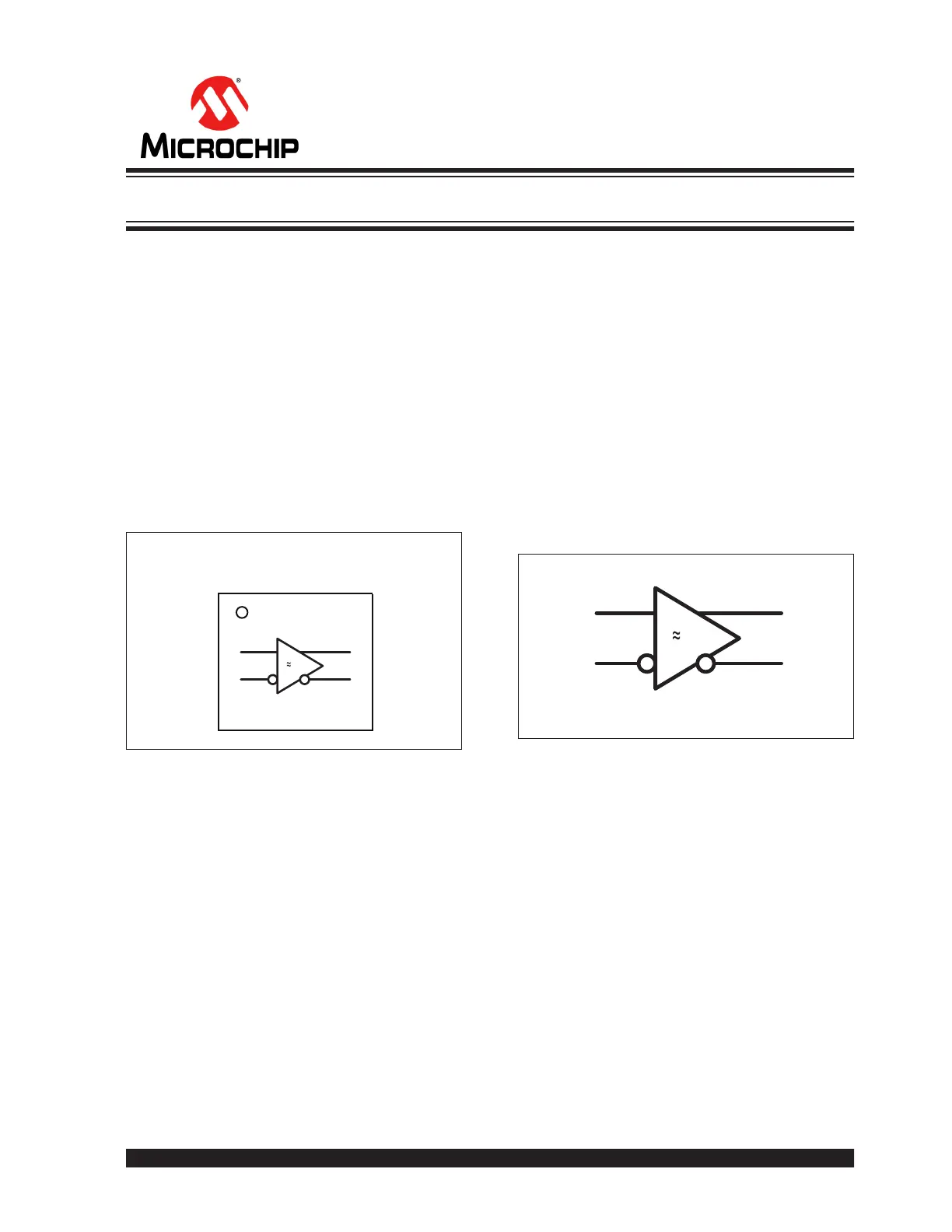
Package Type
SY89206V
8-Lead DFN
NC
D
/D
VBB
VCC
Q
/Q
VEE
1
2
3
4
8
7
6
5
A
V
40V/V
General Description
The SY89206V is a differential PECL/ECL
receiver/buffer in a space-saving (2 mm x 2 mm) DFN
package.
The device is functionally equivalent to the
SY100EL16V, but features a 70% smaller footprint.
The SY89206V provides a VBB output for either
single-ended
use or as a DC bias for AC-coupling to
the device. The VBB pin should be used only as a bias
for the SY89206V as its current sink/source capability
is limited. Whenever used, the VBB pin should be
bypassed with a 0.01 μF capacitor to VCC.
Under open input conditions (pulled to VEE), internal
input clamps will force the Q output LOW
.
Block Diagram
D
/D
Q
/Q
A
V
40V/V
3.3V/5V 1 GHz Differential PECL/ECL Receiver/Buffer
Produktspezifikationen
| Marke: | Microchip |
| Kategorie: | Nicht kategorisiert |
| Modell: | SY89206V |
Brauchst du Hilfe?
Wenn Sie Hilfe mit Microchip SY89206V benötigen, stellen Sie unten eine Frage und andere Benutzer werden Ihnen antworten
Bedienungsanleitung Nicht kategorisiert Microchip

30 Januar 2026
23 Januar 2026
23 Januar 2026
20 Januar 2026
19 Januar 2026
15 Januar 2026
14 Januar 2026
14 Januar 2026
3 Dezember 2025
2 Dezember 2025
Bedienungsanleitung Nicht kategorisiert
Neueste Bedienungsanleitung für -Kategorien-
3 April 2026
3 April 2026
3 April 2026
3 April 2026
3 April 2026
3 April 2026
3 April 2026
3 April 2026
3 April 2026
3 April 2026