Microchip SY89542U Bedienungsanleitung
Microchip Nicht kategorisiert SY89542U
Lies die bedienungsanleitung für Microchip SY89542U (10 Seiten) kostenlos online; sie gehört zur Kategorie Nicht kategorisiert. Dieses Handbuch wurde von 11 Personen als hilfreich bewertet und erhielt im Schnitt 4.7 Sterne aus 2 Bewertungen. Hast du eine Frage zu Microchip SY89542U oder möchtest du andere Nutzer dieses Produkts befragen? Stelle eine Frage
Seite 1/10
1
Precision Edge
®
SY89542U
Micrel, Inc.
M9999-082407
[email protected] or (408) 955-1690
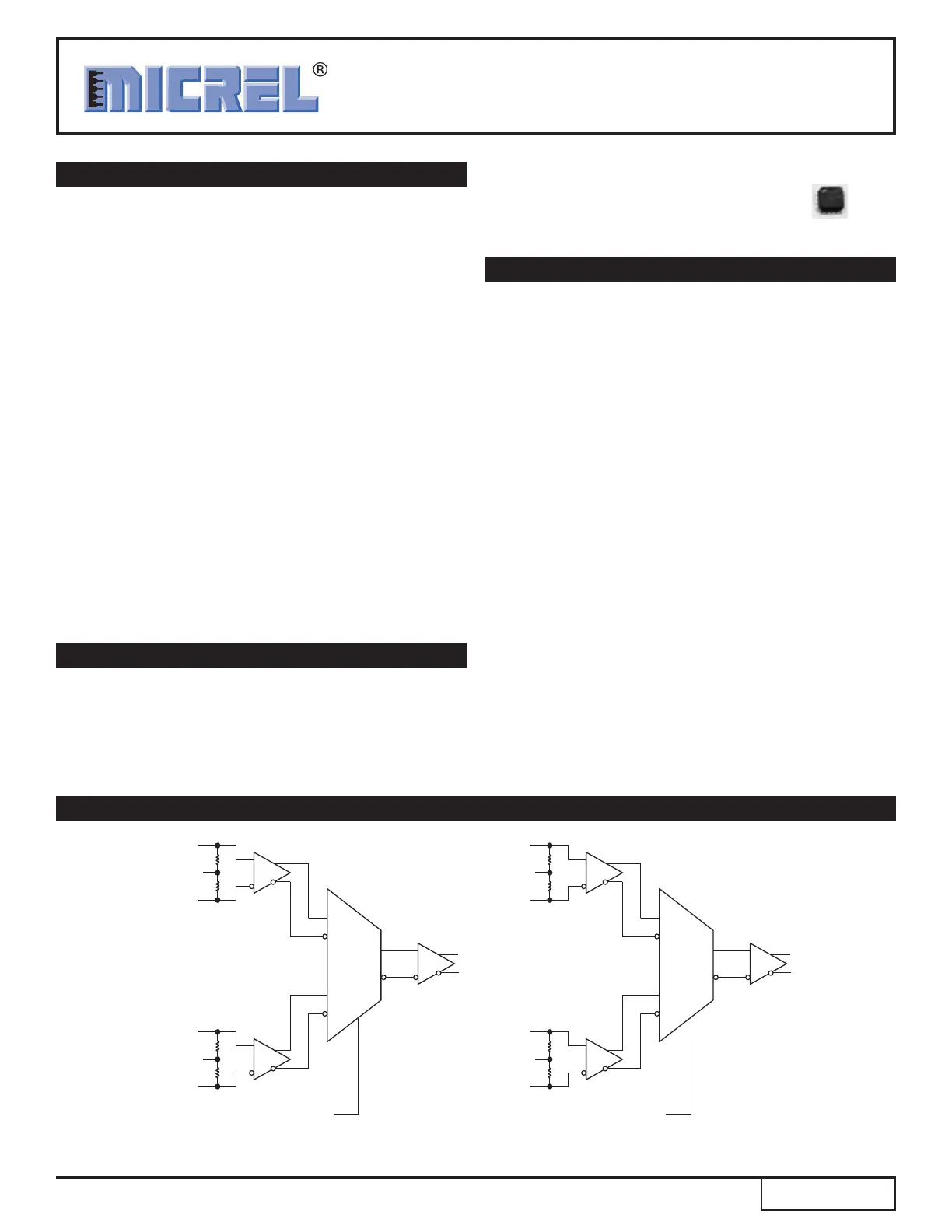
FUNCTIONAL BLOCK DIAGRAM
DESCRIPTION
■Dual 2:1 multiplexer
■Guaranteed AC performance over temp and voltage:
•DC-to > 3.2Gbps data rate throughput
•< 600ps In-to-Out t
pd
•< 150ps t
r
/t
f
■Ultra-low jitter design:
•< 1ps
RMS
random jitter
•< 10ps
PP
deterministic jitter
•< 10ps
PP
total jitter (clock)
•< 0.7ps
RMS
crosstalk-induced jitter
■Unique input isolation design minimizes crosstalk
■Internal input termination
■Unique input termination and V
T
pin accepts
DC-Coupled and AC-coupled inputs (LVDS, LVPECL,
CML)
■350mV LVDS output swing
■CMOS/TTL compatible MUX select
■Power supply 2.5V ±5%
■–40°C to +85°C temperature range
■Available in 32-pin (5mm x 5mm) MLF
®
package
FEATURES
2.5V, 3.2Gbps DUAL, DIFFERENTIAL
2:1 LVDS MULTIPLEXER WITH
INTERNAL TERMINATION
Precision Edge
®
SY89542U
APPLICATIONS
■Redundant clock/data switchover
■SONET/SDH multi-channel select applications
■Fibre Channel applications
■GigE applications
Rev.: DAmendment: /0
Issue Date:August 2007
The SY89542U includes two precision, high-speed 2:1
differential Muxes with LVDS (350mV) compatible outputs
with a guaranteed data rate throughput of 3.2Gbps over
temperature and voltage.
The SY89542U differential inputs include a unique, 3-pin
internal termination that allows access to the termination
network through a V
T
pin. This feature allows the device to
easily interface to different logic standards, both AC- and
DC-coupled without external resistor-bias and termination
networks. The result is a clean, stub-free, low jitter interface
solution.
The SY89542U operates from a single 2.5V supply, and
is guaranteed over the full industrial temperature range
(–40°C to +85°C). For applications that require a 3.3V supply,
consider the SY89543L. The SY89542U is part of Micrel’s
Precision Edge
®
product family.
All support documentation can be found on Micrel’s web
site at www.micrel.com.
Precision Edge
®
LVDS
QA
/QA
INA0
/INA0
V
TA0
50Ω
50Ω
0
MUX A
2:1 MUX
1
INA1
/INA1
V
TA1
50Ω
50Ω
S
SELA (CMOS/TTL)
LVDS
QB
/QB
INB0
/INB0
V
TB0
50Ω
50Ω
0
MUX B
2:1 MUX
1
INB1
/INB1
V
TB1
50Ω
50Ω
S
SELB (CMOS/TTL)
Precision Edge is a registered trademark of Micrel, Inc.
Micro
LeadFrame and MLF are registered trademarks of Amkor Technology, Inc.
Produktspezifikationen
| Marke: | Microchip |
| Kategorie: | Nicht kategorisiert |
| Modell: | SY89542U |
Brauchst du Hilfe?
Wenn Sie Hilfe mit Microchip SY89542U benötigen, stellen Sie unten eine Frage und andere Benutzer werden Ihnen antworten
Bedienungsanleitung Nicht kategorisiert Microchip

30 Januar 2026
23 Januar 2026
23 Januar 2026
20 Januar 2026
19 Januar 2026
15 Januar 2026
14 Januar 2026
14 Januar 2026
3 Dezember 2025
2 Dezember 2025
Bedienungsanleitung Nicht kategorisiert
Neueste Bedienungsanleitung für -Kategorien-
3 April 2026
3 April 2026
3 April 2026
3 April 2026
3 April 2026
3 April 2026
3 April 2026
3 April 2026
3 April 2026
3 April 2026