Microchip SY89828L Bedienungsanleitung
Microchip Nicht kategorisiert SY89828L
Lies die bedienungsanleitung für Microchip SY89828L (13 Seiten) kostenlos online; sie gehört zur Kategorie Nicht kategorisiert. Dieses Handbuch wurde von 4 Personen als hilfreich bewertet und erhielt im Schnitt 4.5 Sterne aus 7 Bewertungen. Hast du eine Frage zu Microchip SY89828L oder möchtest du andere Nutzer dieses Produkts befragen? Stelle eine Frage
Seite 1/13
1
Precision Edge
®
SY89828L
MicreL, Inc.
M9999-012208
[email protected] or (408) 955-1690
DESCRIPTION
■High-performance dual 1:10, 1GHz LVDS fanout
buffer/translator
■Two banks of 10 differential LVDS outputs
■Guaranteed AC parameters over temperature and
voltage:
•> 1GHz f
MAX
•< 50ps within device skew
•< 400ps t
r
, t
f
time
■Each bank includes a 2:1 input mux
■2:1 mux input accepts LVDS and LVPECL
■Low jitter performance
•< 1ps
RMS
cycle-to-cycle jitter
•< 1ps
PP
total jitter
■3.3V supply voltage
■Output enable function
■LVDS input includes internal 100Ω termination
■Available in a 64-Pin EPAD-TQFP
FEATURES
3.3V 1GHz DUAL 1:10 PRECISION
LVDS FANOUT BUFFER/
TRANSLATOR WITH 2:1 INPUT MUX
Precision Edge
®
SY89828L
APPLICATIONS
■Enterprise networking
■High-end servers
■Communications
Rev.: DAmendment: /0
Issue Date:January 2008
The SY89828L is a precision fanout buffer with 20
differential LVDS (Low Voltage Differential Swing) output
pairs. The part is designed for use in low voltage 3.3V
applications that require a large number of outputs to drive
precisely aligned, ultra low-skew signals to their destination.
The input is multiplexed from either LVDS or LVPECL (Low
Voltage Positive Emitter Coupled Logic) by the CLK_SEL1
and CLK_SEL2 pins. The Output Enables (OE1 and OE2)
are synchronous so that the outputs will only be enabled/
disabled when they are already in the LOW state. This
avoids any chance of generating a runt clock pulse when
the device is enabled/disabled as can happen with an
asynchronous control.
The SY89828L features a low pin-to-pin skew of less
than 50ps—performance previously unachievable in a
standard product having such a high number of outputs.
The SY89828L is available in a single space saving package,
enabling a lower overall cost solution.
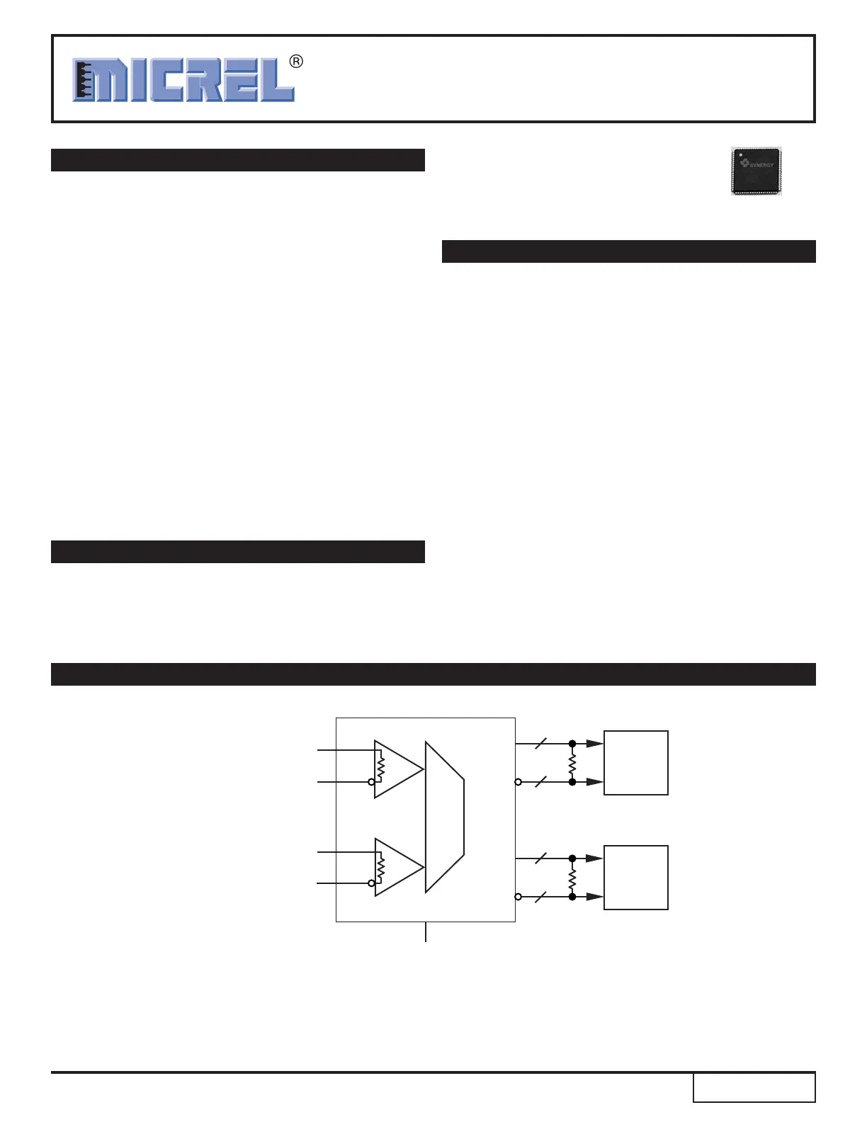
TYPICAL APPLICATION CIRCUIT
SEL1
Primary/Backup Clock Select
(Switchover with 2.0ns)
LVDS_CLKA
/LVDS_CLKA
LVDS_CLKB
/LVDS_CLKB
Primary Clock Source
Backup Clock Source
5
5
5
5
100Ω
100Ω
Primary
Card
Redundant
Card
System using SY89828L as a switchover circuit from a Primary Clock to a Redundant backup Clock in a fail-safe application.
LVPECL inputs not shown in this application.
Precision Edge is a registered trademark of Micrel, Inc.
Precision Edge
®
Produktspezifikationen
| Marke: | Microchip |
| Kategorie: | Nicht kategorisiert |
| Modell: | SY89828L |
Brauchst du Hilfe?
Wenn Sie Hilfe mit Microchip SY89828L benötigen, stellen Sie unten eine Frage und andere Benutzer werden Ihnen antworten
Bedienungsanleitung Nicht kategorisiert Microchip

30 Januar 2026
23 Januar 2026
23 Januar 2026
20 Januar 2026
19 Januar 2026
15 Januar 2026
14 Januar 2026
14 Januar 2026
3 Dezember 2025
2 Dezember 2025
Bedienungsanleitung Nicht kategorisiert
Neueste Bedienungsanleitung für -Kategorien-
3 April 2026
3 April 2026
3 April 2026
3 April 2026
3 April 2026
3 April 2026
3 April 2026
3 April 2026
3 April 2026
3 April 2026