Microchip SY89847U Bedienungsanleitung
Microchip Nicht kategorisiert SY89847U
Lies die bedienungsanleitung für Microchip SY89847U (24 Seiten) kostenlos online; sie gehört zur Kategorie Nicht kategorisiert. Dieses Handbuch wurde von 12 Personen als hilfreich bewertet und erhielt im Schnitt 4.1 Sterne aus 2 Bewertungen. Hast du eine Frage zu Microchip SY89847U oder möchtest du andere Nutzer dieses Produkts befragen? Stelle eine Frage
Seite 1/24
2018 Microchip Technology Inc.DS20006101A-page 1
SY89847U
Features
•Selects Between Two Sources and Provides 5
Precision LVDS Copies
•Fail Safe Input Prevents Outputs from Oscillating
when Input is Invalid
•Guaranteed AC Performance over Temperature
and Supply Voltage:
-DC-to >1.5GHz Throughput
-<1000ps Propagation Delay (IN-to-Q)
-<210ps Rise/Fall Times
•Ultra-Low Jitter Design:
-<1ps
RMS
Random Jitter
-<1ps
RMS
Cycle-to-Cycle Jitter
-<10ps
PP
Total Jitter (Clock)
-<0.7ps
RMS
MUX Crosstalk Induced Jitter
•Unique, Patented MUX Input Isolation Design
Minimizes Adjacent Channel Crosstalk
•Unique, Patented Internal Termination and V
T
Pin
Accepts DC- and AC-Coupled Inputs (CML,
PECL, LVDS)
•Wide Input Voltage Range V
CC
to GND
•2.5V ±5% Supply Voltage
•–40°C to +85°C Industrial Temperature Range
•Available in 32-Pin (5mm x 5mm) QFN Package
Applications
•Fail Safe Clock Protection
•Ultra-Low Jitter LVDS Clock Distribution
•Rack-Based Telecom/Datacom
Markets
•LAN/WAN
•Enterprise Servers
•ATE
•Test and Measurement
General Description
The SY89847U is a 2.5V, 1:5 LVDS fanout buffer with a
2:1 differential input multiplexer (MUX). A unique fail
safe input (FSI) protection prevents metastable output
conditions when the selected input clock fails to a DC
voltage (voltage between the pins of the differential
input drops significantly below 100mV).
The differential input includes Microchip’s unique, 3-pin
internal termination architecture that can interface to
any differential signal (AC- or DC-coupled) as small as
100mV (200mV
PP
) without any level shifting or
termination resistor networks in the signal path. The
outputs are LVDS compatible with very fast rise/fall
times guaranteed to be less than 210ps.
The SY89847U operates from a 2.5V ±5% supply and
is guaranteed over the full industrial temperature range
of –40°C to +85°C. The SY89847U is part of
Microchip’s high-speed, Precision Edge
®
product line.
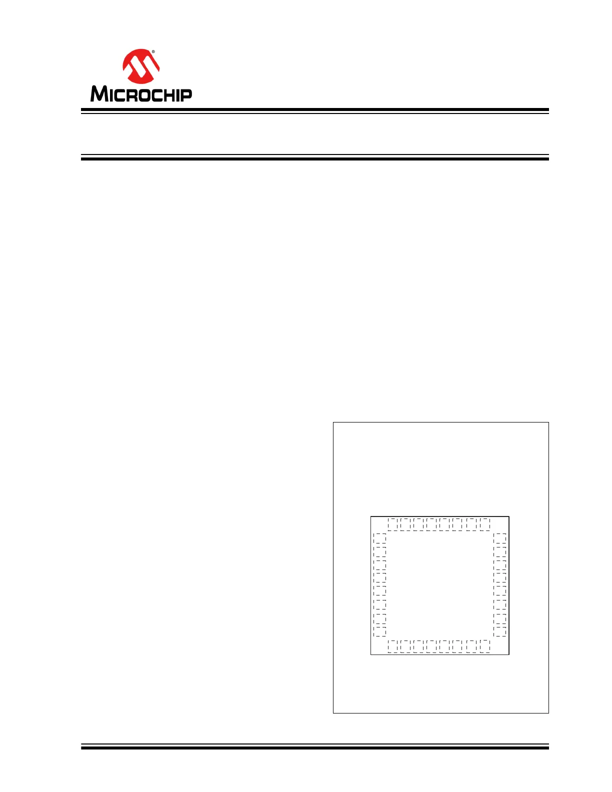
Package Type
SY89847U
5mm x 5mm QFN-32 (M)
(Top View)
VT0
IN0
/IN0
OE
SEL
IN1
/IN1
VT1
VCC
VCC
GND
GND
VREF-AC1
/Q4
Q4
VCC
1
2
3
4
5
6
7
8
9101112131415
16
24
23
22
21
20
19
18
17
32313029282726
25
Q1
/Q1
VCC
Q2
/Q2
VCC
Q3
/Q3
VCC
VCC
GND
GND
VREF-AC0
Q0
/Q0
VCC
1.5GHz Precision LVDS 1:5 Fanout with 2:1 MUX
and Fail Safe Input with Internal Termination
Produktspezifikationen
| Marke: | Microchip |
| Kategorie: | Nicht kategorisiert |
| Modell: | SY89847U |
Brauchst du Hilfe?
Wenn Sie Hilfe mit Microchip SY89847U benötigen, stellen Sie unten eine Frage und andere Benutzer werden Ihnen antworten
Bedienungsanleitung Nicht kategorisiert Microchip

30 Januar 2026
23 Januar 2026
23 Januar 2026
20 Januar 2026
19 Januar 2026
15 Januar 2026
14 Januar 2026
14 Januar 2026
3 Dezember 2025
2 Dezember 2025
Bedienungsanleitung Nicht kategorisiert
Neueste Bedienungsanleitung für -Kategorien-
3 April 2026
3 April 2026
3 April 2026
3 April 2026
3 April 2026
3 April 2026
3 April 2026
3 April 2026
3 April 2026
3 April 2026