Microchip SY89875U Bedienungsanleitung
Microchip Nicht kategorisiert SY89875U
Lies die bedienungsanleitung für Microchip SY89875U (10 Seiten) kostenlos online; sie gehört zur Kategorie Nicht kategorisiert. Dieses Handbuch wurde von 10 Personen als hilfreich bewertet und erhielt im Schnitt 4.3 Sterne aus 5 Bewertungen. Hast du eine Frage zu Microchip SY89875U oder möchtest du andere Nutzer dieses Produkts befragen? Stelle eine Frage
Seite 1/10
1
Precision Edge
®
SY89875U
Micrel, Inc.
M9999-082407
[email protected] or (408) 955-1690
DESCRIPTION
Integrated programmable clock divider and 1:2
fanout buffer
Guaranteed AC performance over temperature and
voltage:
•> 2.0GHz f
MAX
•< 200ps t
r
/t
f
•< 15ps within device skew
Low jitter design:
•<10ps
PP
total jitter
•<1ps
RMS
cycle-to-cycle jitter
Unique input termination and V
T
Pin for DC-coupled
and AC-coupled Inputs;CML, PECL, LVDS and
HSTL
LVDS compatible outputs
TTL/CMOS inputs for select and reset
Parallel programming capability
Programmable divider ratios of 1, 2, 4, 8 and 16
Low voltage operation 2.5V
Output disable function
–40°C to 85°C temperature range
Available in 16-pin (3mm x 3mm) MLF
®
package
FEATURES
2.5V, 2.0GHz ANY DIFF. IN-TO-LVDS
PROGRAMMABLE CLOCK DIVIDER AND 1:2
FANOUT BUFFER W/ INTERNAL TERMINATION
Precision Edge
®
SY89875U
APPLICATIONS
SONET/SDH line cards
Transponders
High-end, multiprocessor servers
Rev.: DAmendment: /0
Issue Date:August 2007
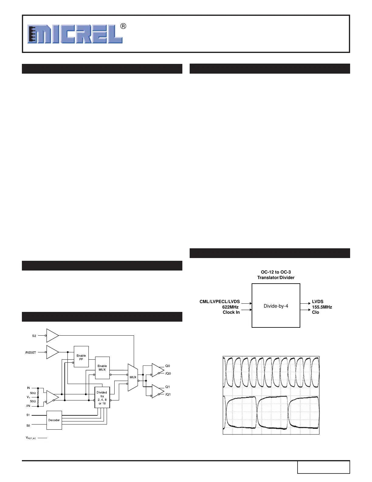
This low-skew, low-jitter device is capable of accepting a
high-speed (e.g., 622MHz or higher) CML, LVPECL, LVDS
or HSTL clock input signal and dividing down the frequency
using a programmable divider to create a lower speed
version of the input clock. Available divider ratios are 2, 4, 8
and 16, or straight pass-through.
The differential input buffer has a unique internal
termination design that allows access to the termination
network through a V
T
pin. This feature allows the device to
easily interface to different logic standards. A V
REF-AC
reference is included for AC-coupled applications.
The /RESET input asynchronously resets the divider. In
the pass-through function (divide by 1) the /RESET
synchronously enables or disables the outputs on the next
falling edge of IN (rising edge of /IN).
FUNCTIONAL BLOCK DIAGRAM
TYPICAL PERFORMANCE
9
9
!
"#$
"#$
!
%
Divide-by-4
C
ML/LVPECL/LVDS
622MHz
Clock In
OC-12 to OC-3
Translator/Divider
LVDS
155.5MH
z
Clock Ou
t
622MHz In
/
Q0
Q0
/IN
IN
155.5MHz Out
Precision Edge is a registered trademark of Micrel, Inc.
MicroLeadFrame and MLF are registered trademarks of Amkor Technology, Inc.
Produktspezifikationen
| Marke: | Microchip |
| Kategorie: | Nicht kategorisiert |
| Modell: | SY89875U |
Brauchst du Hilfe?
Wenn Sie Hilfe mit Microchip SY89875U benötigen, stellen Sie unten eine Frage und andere Benutzer werden Ihnen antworten
Bedienungsanleitung Nicht kategorisiert Microchip

30 Januar 2026
23 Januar 2026
23 Januar 2026
20 Januar 2026
19 Januar 2026
15 Januar 2026
14 Januar 2026
14 Januar 2026
3 Dezember 2025
2 Dezember 2025
Bedienungsanleitung Nicht kategorisiert
Neueste Bedienungsanleitung für -Kategorien-
3 April 2026
3 April 2026
3 April 2026
3 April 2026
3 April 2026
3 April 2026
3 April 2026
3 April 2026
3 April 2026
3 April 2026