Texas Instruments ADC3908S065 Bedienungsanleitung
Texas Instruments Nicht kategorisiert ADC3908S065
Lies die bedienungsanleitung für Texas Instruments ADC3908S065 (47 Seiten) kostenlos online; sie gehört zur Kategorie Nicht kategorisiert. Dieses Handbuch wurde von 9 Personen als hilfreich bewertet und erhielt im Schnitt 5.0 Sterne aus 8 Bewertungen. Hast du eine Frage zu Texas Instruments ADC3908S065 oder möchtest du andere Nutzer dieses Produkts befragen? Stelle eine Frage
Seite 1/47
ADC3908Dx and ADC3908Sx 8-bit, 25 to 125MSPS Low Latency, Low Power, Small,
Single and Dual Channel ADC with Integrated Input Buffers
1 Features
•Sampling rate up to 125MSPS
•Latency: 1 clock cycle
•Low power (2 channel):
–90mW at 125MSPS
–56mW at 25MSPS
–3mW in PD mode
•Small footprint: 32-VQFN (4mm x 4mm)
•Single or dual channel ADC
•Internal reference
•No missing codes, ±0.25 LSB INL
•Buffered, differential or single ended inputs
•Input bandwidth: 150MHz (3dB)
•Single 1.8V supply
–Optional 3.3V
IO
capability
•Industrial temperature range: -40°C to 105°C
•Parallel (SDR, DDR) CMOS interface
•Spectral performance (FS
CLK
= 125MSPS, f
IN
= 5
MHz):
–SNR: 49.8dBFS
–SFDR: 60dBFS
2 Applications
•Low latency control loops
•Laser scanners
•Displacement sensors
•Detection equipment
3 Description
The ADC3908Dx and ADC3908Sx are a family
of ultra-low power 8-bit 125MSPS high-speed dual
and single channel analog-to-digital converters. High-
speed control loops benefit from the short latency of
only 1 clock cycle. The ADC consumes only 90mW at
125MSPS with a power consumption that scales with
lower sampling rates.
The ADC3908Dx and ADC3908Sx uses parallel DDR
or SDR CMOS interface to output the data, and can
be driven at +1.8V or +3.3V to accommodate various
receiver requirements. The analog input and output
interface can be easily configured via pin control
(Interface Configuration Table). The device is a pin-
to-pin compatible family of ADCs with 8 and 10-bit
resolution and different speed grades. The device is
available in a 32-pin VQFN package, and supports
industrial temperature range from -40 to +105°C.
Package Information
PART NUMBERPACKAGE
(1)
PACKAGE SIZE
(2)
ADC3908D025,
'D065, 'D125
ADC3908S025,'S06
5, 'S125
VQFN (32)4mm × 4mm
(1)For more information, see Section 11.
(2)The package size (length × width) is a nominal value and
includes pins, where applicable.
Device Information
PART NUMBER
(c= #CH; sss= MSPS)
RESOLUTION
SAMPLING RATE
MSPS
ADC3910csss10-Bit25, 65, 125
ADC3908csss8-Bit25, 65, 125
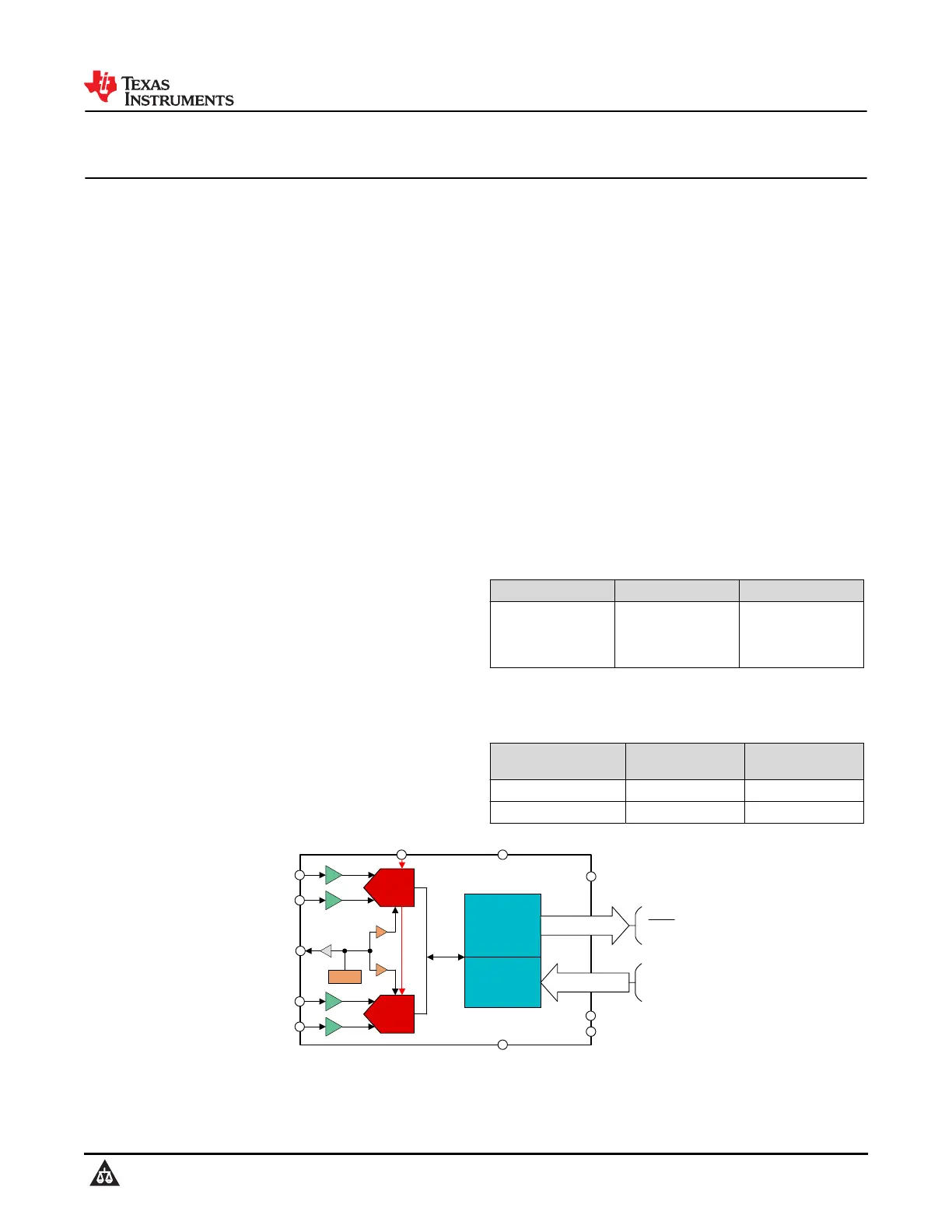
REF
ADC
ADC
Parallel
Interface
Control
Interface
RESET
AVDD
IOVDD
CLK
GND
M2
M1
M0
INAP
INAM
INBP
INBM
VCM
DCLK
DCLK
#8 DOUT
PDN
Block Diagram
ADC3908D025, ADC3908D065, ADC3908D125
ADC3908S025, ADC3908S065, ADC3908S125
SBASAU9 – OCTOBER 2024
An IMPORTANT NOTICE at the end of this data sheet addresses availability, warranty, changes, use in safety-critical applications,
intellectual property matters and other important disclaimers. PRODUCTION DATA.
Produktspezifikationen
| Marke: | Texas Instruments |
| Kategorie: | Nicht kategorisiert |
| Modell: | ADC3908S065 |
Brauchst du Hilfe?
Wenn Sie Hilfe mit Texas Instruments ADC3908S065 benötigen, stellen Sie unten eine Frage und andere Benutzer werden Ihnen antworten
Bedienungsanleitung Nicht kategorisiert Texas Instruments

3 April 2026
3 April 2026
2 April 2026
2 April 2026
2 April 2026
2 April 2026
2 April 2026
2 April 2026
1 April 2026
1 April 2026
Bedienungsanleitung Nicht kategorisiert
Neueste Bedienungsanleitung für -Kategorien-
3 April 2026
3 April 2026
3 April 2026
3 April 2026
3 April 2026
3 April 2026
3 April 2026
3 April 2026
3 April 2026
3 April 2026