Texas Instruments CD74HCT4051 Bedienungsanleitung
Texas Instruments Nicht kategorisiert CD74HCT4051
Lies die bedienungsanleitung für Texas Instruments CD74HCT4051 (50 Seiten) kostenlos online; sie gehört zur Kategorie Nicht kategorisiert. Dieses Handbuch wurde von 4 Personen als hilfreich bewertet und erhielt im Schnitt 4.2 Sterne aus 2 Bewertungen. Hast du eine Frage zu Texas Instruments CD74HCT4051 oder möchtest du andere Nutzer dieses Produkts befragen? Stelle eine Frage
Seite 1/50
CDx4HC405x, CD4HCT405x High-Speed CMOS Logic Analog
Multiplexer and Demultiplexer
1 Features
•Wide analog input voltage range: ±5V maximum
•Low ON-resistance:
–70Ω typical (V
CC
– V
EE
= 4.5V)
–40Ω typical (V
CC
– V
EE
= 9V)
•Low crosstalk between switches
•Fast switching and propagation speeds
•Break-before-make switching
•Wide operating temperature range:
–40°C to +125°C
•Operation control voltage: 4.5V to 5.5V
•Switch voltage: 0V to 10V
•Direct LSTTL input logic compatibility
V
IL
= 0.8V maximum, V
IH
= 2V minimum
•CMOS input compatibility
I
I
≤ 1µA at V
OL
, V
OH
2 Applications
•Digital radio
•Signal gating
•Factory automation
•Televisions
•Appliances
•Programmable logic circuits
•Sensors
3 Description
The CDx4HC405x and CDx4HCT405x device is a
digitally controlled analog switch that uses silicon
gate CMOS technology to achieve operating speeds
similar to LSTTL with the low-power consumption of
standard CMOS integrated circuits.
This analog multiplexer and demultiplexer controls
analog voltages that may vary across the voltage
supply range (for example, V
CC
to V
EE
). It is a
bidirectional switch that allows any analog input to be
used as an output and vice versa. The switch has low
ON resistance and low OFF leakages. In addition, this
device has an enable control that, when high, disables
all switches to their OFF state.
Device Information
PART NUMBERT
A
PACKAGE
(1)
PACKAGE SIZE
(2)
CD54HCx405x
-55°C to 125°C
J (CDIP, 16)19.56mm × 6.92mm
CD74HCx405x
N (PDIP, 16)19.30mm × 6.35mm
D (SOIC, 16)9.9mm × 3.9mm
NS (SOP, 16)10.3mm × 5.3mm
PW (TSSOP, 16)5mm × 4.4mm
(1)For more information, see Section 11.
(2)The package size (length × width) is a nominal value and
includes pins, where applicable.
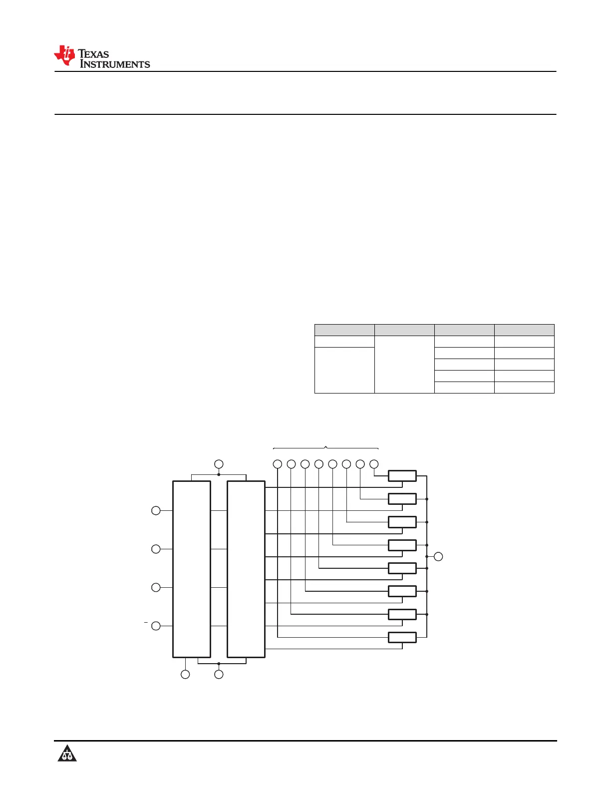
TG
TG
TG
TG
TG
TG
TG
3
A
COMMO
N
OUT/IN
BINARY
TO
1 OF 8
DECODER
WITH
ENABLE
11
10
9
6E
S
2
S
1
S
0
LOGIC
LEVEL
CONVERSION
87
GNDV
EE
16
V
CC
131415121524
AAAAAAAA
76543210
CHANNELIN/OUT
TG
Functional Diagram of HCT4051
CD54HC4051, CD74HC4051, CD54HCT4051, CD74HCT4051, CD54HC4052, CD74HC4052,
CD54HCT4052, CD74HCT4052, CD54HC4053, CD74HC4053, CD54HCT4053, CD74HCT4053
SCHS122O – NOVEMBER 1997 – REVISED JANUARY 2026
An IMPORTANT NOTICE at the end of this data sheet addresses availability, warranty, changes, use in safety-critical applications,
intellectual property matters and other important disclaimers. PRODUCTION DATA.
Produktspezifikationen
| Marke: | Texas Instruments |
| Kategorie: | Nicht kategorisiert |
| Modell: | CD74HCT4051 |
Brauchst du Hilfe?
Wenn Sie Hilfe mit Texas Instruments CD74HCT4051 benötigen, stellen Sie unten eine Frage und andere Benutzer werden Ihnen antworten
Bedienungsanleitung Nicht kategorisiert Texas Instruments

3 April 2026
3 April 2026
2 April 2026
2 April 2026
2 April 2026
2 April 2026
2 April 2026
2 April 2026
1 April 2026
1 April 2026
Bedienungsanleitung Nicht kategorisiert
Neueste Bedienungsanleitung für -Kategorien-
3 April 2026
3 April 2026
3 April 2026
3 April 2026
3 April 2026
3 April 2026
3 April 2026
3 April 2026
3 April 2026
3 April 2026