Texas Instruments LMK1C1104 Bedienungsanleitung
Texas Instruments Nicht kategorisiert LMK1C1104
Lies die bedienungsanleitung für Texas Instruments LMK1C1104 (26 Seiten) kostenlos online; sie gehört zur Kategorie Nicht kategorisiert. Dieses Handbuch wurde von 14 Personen als hilfreich bewertet und erhielt im Schnitt 4.0 Sterne aus 5 Bewertungen. Hast du eine Frage zu Texas Instruments LMK1C1104 oder möchtest du andere Nutzer dieses Produkts befragen? Stelle eine Frage
Seite 1/26
LMK1C110x 1.8-V, 2.5-V, and 3.3-V LVCMOS Clock Buffer Family
1 Features
•High-performance 1:2, 1:3 or 1:4 LVCMOS clock
buffer
•Very low output skew < 50 ps
•Extremely low additive jitter < 50 fs maximum
–7.5 fs typical at V
DD
= 3.3 V
–10 fs typical at V
DD
= 2.5 V
–19.2 fs typical at V
DD
= 1.8 V
•Very low propagation delay < 3 ns
•Synchronous output enable
•Supply voltage: 3.3 V, 2.5 V, or 1.8 V
–3.3-V tolerant input at all supply voltages
–Fail-safe inputs
•f
max
= 250 MHz for 3.3 V
f
max
= 200 MHz for 2.5 V and 1.8 V
•Operating temperature range: –40°C to 125°C
•Available in 8-pin TSSOP package
•Available in 8-pin WSON package
2 Applications
•Factory automation & control
•Telecommunications equipment
•Data center & enterprise computing
•Grid infrastructure
•Motor drives
•Medical imaging
3 Description
The LMK1C110x is a modular, high-performance, low-
skew, general-purpose clock buffer family from Texas
Instruments. The entire family is designed with a
modular approach in mind. Three different fan-out
variations, 1:2, 1:3, 1:4, are available.
All of the devices within this family are pin-compatible
to each other and backwards compatible to the
CDCLVC110x family for easy handling.
All family members share the same high performing
characteristics such as low additive jitter, low skew,
and wide operating temperature range.
The LMK1C110x supports a synchronous output
enable control (1G) which switches the outputs into
a low state when 1G is low. These devices have a
fail-safe input that prevents oscillation at the outputs
in the absence of an input signal and allows for input
signals before VDD is supplied.
The LMK1C110x family operates in a 1.8-V, 2.5-V and
3.3-V environment and are characterized for operation
from –40°C to 125°C.
Device Information
(1)
PART NUMBERPACKAGEBODY SIZE (NOM)
LMK1C1102
TSSOP (8)3.00 mm × 4.40 mmLMK1C1103
LMK1C1104
LMK1C1102
WSON (8)2.00 mm × 2.00 mm
LMK1C1104
(1)For all available packages, see the orderable addendum at
the end of the data sheet.
LVCMOSLVCMOS
LVCMOS
LVCMOS
LVCMOS
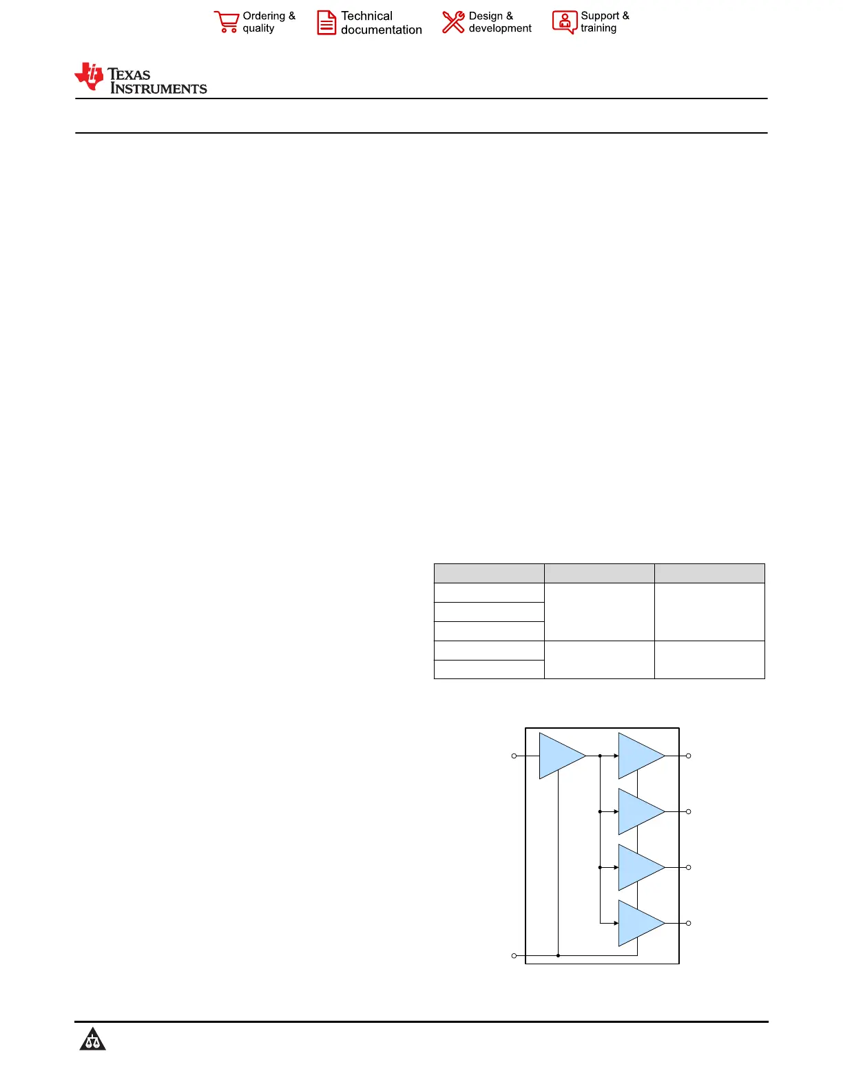
CLKIN
1G
Y0
Y1
Y2
Y3
Functional Block Diagram
LMK1C1102, LMK1C1103, LMK1C1104
SNAS791D – DECEMBER 2019 – REVISED FEBRUARY 2022
An IMPORTANT NOTICE at the end of this data sheet addresses availability, warranty, changes, use in safety-critical applications,
intellectual property matters and other important disclaimers. PRODUCTION DATA.
Produktspezifikationen
| Marke: | Texas Instruments |
| Kategorie: | Nicht kategorisiert |
| Modell: | LMK1C1104 |
Brauchst du Hilfe?
Wenn Sie Hilfe mit Texas Instruments LMK1C1104 benötigen, stellen Sie unten eine Frage und andere Benutzer werden Ihnen antworten
Bedienungsanleitung Nicht kategorisiert Texas Instruments

3 April 2026
3 April 2026
2 April 2026
2 April 2026
2 April 2026
2 April 2026
2 April 2026
2 April 2026
1 April 2026
1 April 2026
Bedienungsanleitung Nicht kategorisiert
Neueste Bedienungsanleitung für -Kategorien-
3 April 2026
3 April 2026
3 April 2026
3 April 2026
3 April 2026
3 April 2026
3 April 2026
3 April 2026
3 April 2026
3 April 2026