Texas Instruments LMS3655-Q1 Bedienungsanleitung
Texas Instruments Nicht kategorisiert LMS3655-Q1
Lies die bedienungsanleitung für Texas Instruments LMS3655-Q1 (61 Seiten) kostenlos online; sie gehört zur Kategorie Nicht kategorisiert. Dieses Handbuch wurde von 2 Personen als hilfreich bewertet und erhielt im Schnitt 4.1 Sterne aus 6 Bewertungen. Hast du eine Frage zu Texas Instruments LMS3655-Q1 oder möchtest du andere Nutzer dieses Produkts befragen? Stelle eine Frage
Seite 1/61
LMS3635-Q1 3.5-A, LMS3655-Q1 5.5-A, 36-V Synchronous, 400-kHz Step-Down
Converter
1 Features
•AEC-Q100-qualified for automotive applications
–Device temperature grade 1: –40°C to +125°C
ambient operating temperature
–Device HBM classification level 2
–Device CDM classification level C6
•96% Peak efficiency while converting 12 V to 5 V
•Low EMI and minimized switch node ringing
•400-kHz (±10%) fixed switching frequency
•–40°C to +150°C junction temperature range
•External frequency synchronization
•RESET output with internal filter and 3-ms release
timer
•Automatic light load mode for improved efficiency
•Pin-selectable forced PWM mode
•Built-In compensation, soft start, current limit,
thermal shutdown, and UVLO
•0.35-V dropout with 3.5-A Load at 25°C (Typical)
•18-µA I
Q_VIN
: quiescent current at 3.3 V
OUT
and no
load (typical)
•Output voltage: 5 V, 3.3 V, and ADJ (1 V to 20 V)
•±1.5% reference voltage tolerance
•Create a custom design using the LMS3655-Q1
with the WEBENCH
®
Power Designer
2 Applications
•Automotive USB charge
•Driver monitoring
•Surround view system ECU
•Mechanically scanning LIDAR
•Vehicle to vehicle
3 Description
The LMS3635-Q1 and LMS3655-Q1 synchronous
buck regulators are optimized for high performance
applications, providing an output voltage of 3.3 V, 5
V, or an adjustable output of 1 V to 20 V. Seamless
transition between PWM and PFM modes, along with
a low quiescent current, ensures high efficiency and
superior transient responses at all loads.
Advanced high-speed circuitry allows the LMS3655-
Q1 to regulate an input of 24 V to an output of 3.3 V
at a fixed frequency of 400 kHz while also enabling
a continuous load current of 5.5 A. An innovative
frequency foldback architecture allows this device to
regulate a 3.3-V output from an input voltage of only
3.5 V. The input voltage can range up to 36 V, with
transient tolerance up to 42 V, easing input surge
protection design.
An open-drain reset output, with built-in filtering and
delay, provides a true indication of system status.
This feature negates the requirement for an additional
supervisory component, saving cost and board space.
Device Information
DEVICE NAMEPACKAGE
(1)
BODY SIZE
LMS3635-Q1
SON (22)4.00 mm × 5.00 mm
LMS3655-Q1
(1)For all available packages, see the orderable addendum at
the end of the data sheet.
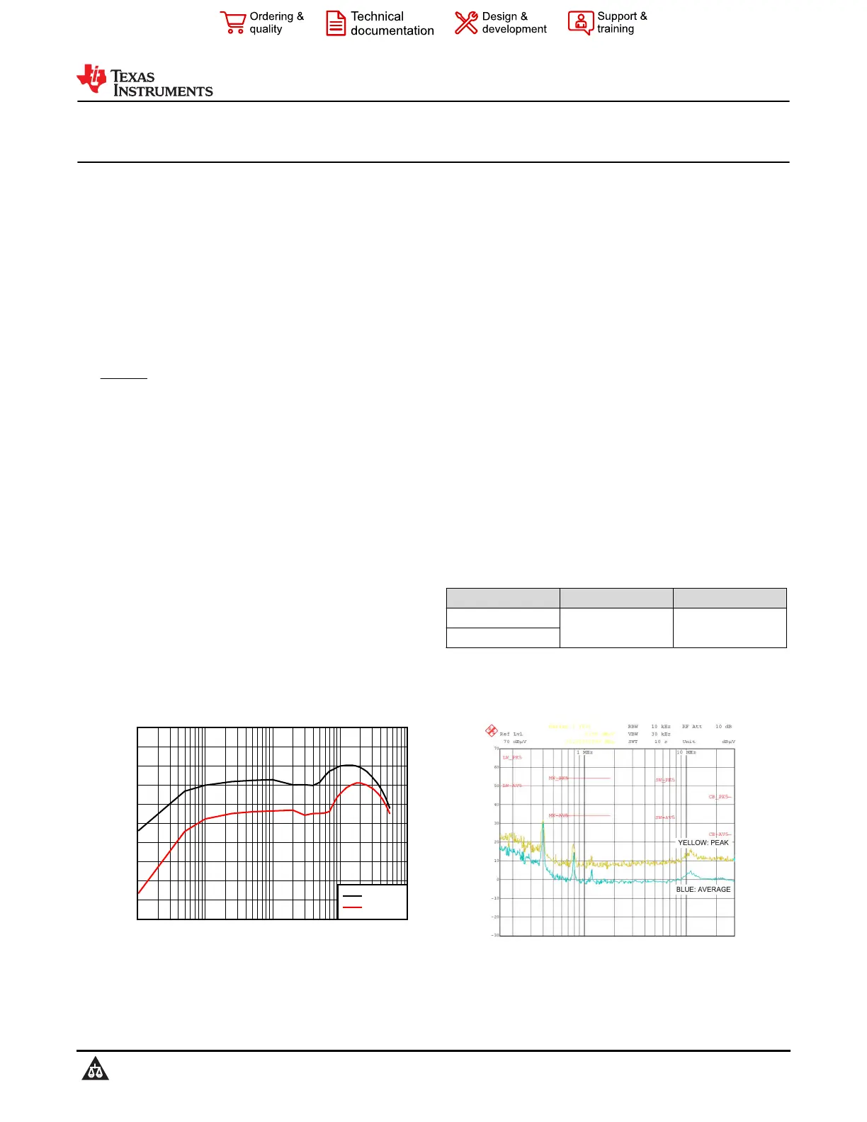
Output Current (A)
Efficiency
0.0010.010.1110
80%
82%
84%
86%
88%
90%
92%
94%
96%
98%
100%
LMS3
V
IN
= 12
V
IN
= 24
LMS3655-Q1 Efficiency: V
OUT
= 5 V
LMS3655-Q1 Conducted EMI: V
OUT = 5 V
, I
OUT
= 5 A
LMS3655-Q1, LMS3635-Q1
SNAS714C – NOVEMBER 2016 – REVISED AUGUST 2021
An IMPORTANT NOTICE at the end of this data sheet addresses availability, warranty, changes, use in safety-critical applications,
intellectual property matters and other important disclaimers. PRODUCTION DATA.
Produktspezifikationen
| Marke: | Texas Instruments |
| Kategorie: | Nicht kategorisiert |
| Modell: | LMS3655-Q1 |
Brauchst du Hilfe?
Wenn Sie Hilfe mit Texas Instruments LMS3655-Q1 benötigen, stellen Sie unten eine Frage und andere Benutzer werden Ihnen antworten
Bedienungsanleitung Nicht kategorisiert Texas Instruments

3 April 2026
3 April 2026
2 April 2026
2 April 2026
2 April 2026
2 April 2026
2 April 2026
2 April 2026
1 April 2026
1 April 2026
Bedienungsanleitung Nicht kategorisiert
Neueste Bedienungsanleitung für -Kategorien-
3 April 2026
3 April 2026
3 April 2026
3 April 2026
3 April 2026
3 April 2026
3 April 2026
3 April 2026
3 April 2026
3 April 2026